�� ��
������
����
�۸�Ϊ�̼��ṩ�IJο��ۣ���ͨ��"��ȡ��ͱ���"
������������������λ~
����
| �ӹ����ƣ��� | Ʒ�ƣ�EVG | �ͺţ�EVG?810 |
| ��;����Բ����ƽ̨ | �Ƿ�羳��Դ���� |
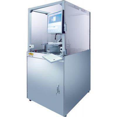
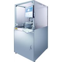
EVG®810LT Series |
LowTemp™ Plasma Activation Systems
 |
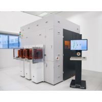
EV Group’s LowTemp (LT) Plasma Activated Bonding is available for both R&D and high volume manufacturing. The EVG LowTemp plasma activation chamber was developed for modular operation. It can be configured as single chamber, stand alone, semi-automated unit (EVG810LT) or integrated in an automated configuration for high volume production (EVG850LT and GEMINI).
The EVG810LT stand alone LowTemp plasma activation system is suitable for applications such as direct bonding for manufacturing of SOI (Silicon-on-Insulator), strained silicon, GeOI (Germanium-on-Insulator) wafers as well as for compound semiconductor applications and MEMS devices.
On the EVG850LT and GEMINI the plasma activation process is the enabling technology for low temperature bonding for CMOS (e.g. imaging sensors, etc.) and Memory (e.g. Flash, SRAM, etc.) applications.
Surface activation for low temperature bonding (fusion/ molecular and intermediate layer bonding)
Fastest kinetics of any wafer bonding mechanism
No wet processes required
Highest bond strength at low temperature annealing (up to 400 °C)
Applicable for SOI, MEMS, compound semiconductors and advanced substrates bonding
High degree of materials compatibility (including CMOS)
Accommodates various substrate chemistries by allowing the use of different process atmospheres: inert gas, oxidizing or reducing gas mixtures
Low process gas consumption
No contamination issues (particle neutral, metal free) Patented technology
Two platform sizes (up to 200mm wafers and up to 300mm wafers)
�����ǿƳ��ͿƼ�����˾ �ֻ��� ��ַ��ɽ�� ��ׯ ������ �������