�� ��
������
����
�۸�Ϊ�̼��ṩ�IJο��ۣ���ͨ��"��ȡ��ͱ���"
������������������λ~
����
| �ӹ����ƣ��� | Ʒ�ƣ�EVG | �ͺţ�20/40/50 |
| ��;��������� | �Ƿ�羳��Դ���� |
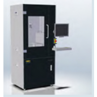
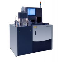
EVG®40(NT) / Alignment Verification Module (AVM)
Versatile metrology for bonding and lithography
The EVG40 (stand-alone tool) and the AVM (HVM-integrated module) enable measurement of lithography relevant parameters like critical dimension, as well as bond alignment accuracy. Because of the high measurement accuracy, it is possible to verify compliance to tight process specifications and instantly optimize integrated process parameters.
In addition to vertical measurement the EVG40 / EVG40NT / AVM also operate at a high resolution in the lateral direction, making them suitable for alignment verification measurements and 3D applications.

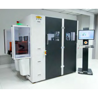
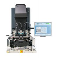
EVG®20 / Infrared Inspection Station
The EVG20 offers a fast inspection method, especially for fusion bonded wafers. A live image of the entire wafer via IR transmission supports void detection down to a radius of 0.5 mm. The infrared inspection system is a perfect match for fusion bonding processes either as the stand-alone EVG20 tool or as a station in EVG’s integrated bonding systems.
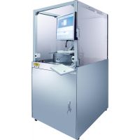
EVG®50 / IMM Key Features
■ Industry leading throughput and resolution multilayer metrology
■ Multi-layer thickness mapping
■ Bond interface inspection
■ Low contact edge handling
■ Particle free
■ Full-area accessible front and back side
■ Self-calibrating for better system reproducibility and more productive time
■ Various output formats
■ *** production inspection for film thickness and thickness variation
Supported Measurement Options:
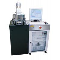
EVG®40(NT) / AVM Key Features
■ Versatile measurement options for lithography and bonding metrology
■ Alignment verification for bonding and lithography
applications
■ Critical dimension (CD) measurement
■ Die-to-die alignment verification
■ Multi-layer thickness measurement
■ High measurement accuracy in vertical and lateral direction
■ High throughput due to specialized calibration routine
■ PC-based measurement and pattern recognition software for highest reliability
�����ǿƳ��ͿƼ�����˾ �ֻ���𐃁𐃂𐃃𐃄𐃅𐃃𐃄𐃃𐃆𐃅𐃄 ��ַ��ɽ�� ��ׯ ������ �������